|
|
|
Silicon is to be deposited on wafers in a LPCVD reactor. We want to
obtain an analytical solution for the silicon deposition rate and reactant concentration
profile for the simplified version of the LPCVD reactor just discussed. Analytical
solutions of this type are important in that an engineer can rapidly gain an understanding
of the important parameters and their sensitivities, without making a number of runs
on the computer. The reaction that is taking place is
|
|
|
|
|
|
|
|
|
|

|
|
|
|
|
|
|
|
|
|
Sections of the reactor are shown in Figures CDE12-10.1 and CDE12-10.2.
|
|
|
|
|
|
|
|
|
|
 Figure CDE12-10.1 Figure CDE12-10.1
 Figure CDE12-10.2 Figure CDE12-10.2
|
|
|
|
|
|
|
|
|
|
1. Balances. In forming our shell balance on the annular region
we shall assume that there are no radial gradients in the annulus and include the
outer tube walls and the boat, which consume some of the reactant by deposition on
the walls in the balance. In addition, we shall neglect any dispersion or diffusion
in the axial direction. Balance on reactant A:
|
|
|
|
|
|
|
|

|
(CDE12-10.1)
|
|
|
|
|
|
|
|
|
Dividing through by and taking the limit as and taking the limit as  0 gives 0 gives
|
|
|
|
|
|
|
|
|
|

|
(CDE12-10.2)
|
|
|
|
|
|
|
Mole balance
on the reacting
gas
|
|
2. Rate laws. The rate of silicon deposition, (mol/ dm 2 (mol/ dm 2 s), is equal to the rate of depletion of SiH 2
. s), is equal to the rate of depletion of SiH 2
.
|
|
|
|
|
|
|
|
|
|

|
(CD12-101)
|
|
|
|
|
|
|
|
|
where the units of C A and k are mol/dm 3
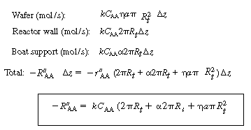
and dm/s, respectively. Deposition takes place on the reactor walls, the
support, and on the wafer surfaces. The corresponding depletion of reactant gas on
each of these surfaces is
|
|
|
|
|
|
|
|
|

|
(CDE12-10.3)
|
|
|
|
|
|
|
Radial
concentration
profile
|
|
Concentration profile and effectiveness factor. From Example
CD12-2 we derived the radial concentration profile between the wafers as
|
|
|
|
|
|
|
|
|
|

|
(CDE12-7.9)
|
|
|
|
|
|
|
|
|
The corresponding effectiveness factor was
|
|
|
|
|
|
|
|
|
|

|
(CDE12-9.12)
|
|
|
|
|
|
|
|
|
4. Concentration profile in the annular region. Combining Equations
(CDE12-10.2) and (CDE12-10.3) yields
|
|
|
|
|
|
|
|
|
|

|
(CDE12-10.4)
|
|
|
|
|
|
|
|
|
Writing F Az
and C AA in
terms of conversion, we have
|
|
|
|
|
|
|
|
Axial
concentration
profile
|
|

|
(CDE12-10.5)
|
|
|
|
where C A0
and F A0 refer to the
reactant concentration and molar flow rates at
the entrance to the reactor.
|
|
|
|
|
|
|
|
|
|
Combining Equations (CDE12-10.4) and (CDE12-10.5) gives
|
|
|
|
|
|
|
|
|
|

|
(CDE12-10.6)
|
|
|
|
|
|
|
|
|
Collecting terms, we can obtain an expression involving the Damköhler
number, Da:
|
|
|
|
|
|
|
|
|
|

|
(CDE12-10.7)
|
|
|
|
|
|
|
|
|
where

|
|
|
|
|
|
|
|
|
|
Solving for conversion as a function of distance along the length
of the reactor yields
|
|
|
|
|
|
|
|
|
|

|
(CDE12-10.8)
|
|
|
|
|
|
|
|
|
or, in terms of concentration,
|
|
|
|
|
|
|
|
|
|

|
(CDE12-10.9)
|
|
|
|
|
|
|
|
|
The deposition rate as a function of r and z can now
be obtained as follows. The deposition rate at a location r and is is
|
|
|
|
|
|
|
|
|
|

|
(CDE12-10.10)
|
|
|
|
|
|
|
|
|
First, using Equation (CDE12-2.9) to relate C A
(r, z) and C AA
(z), we obtain
|
|
|
|
|
|
|
|
|
|

|
|
|
|
|
|
|
|
|
|
Next, we use Equation (CDE12-3.9) to determine the rate as a function
of distance down the reactor.
|
|
|
|
|
|
|
|
|
|

|
(CDE12-10.11)
|
|
|
|
|
|
|
|
|
The thickness,T, of the deposit is obtained by integrating
the deposition rate with respect to time,
|
|
|
|
|
|
|
|
|
|

|
|
|
|
|
|
|
|
|
|
where r is the molar density of the material deposited, g mol/cm
3 .
The 2 accounts for deposition on both sides of the wafer. Integrating, we obtain
|
|
|
|
|
|
|
|
|
|

|
(CDE12-10.12)
|
|
|
|
|
|
|
|
|
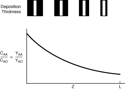
The reactant concentration profile and deposition thickness along
the length of the reactor are shown schematically in Figure CDE12-10.3 for the case
of small values of the Thiele modulus
|
|
|
|
|
|
|
|
|
|
 Figure 12-10.3 Figure 12-10.3
|
|

 Figure CDE12-10.1
 Figure CDE12-10.2

 and taking the limit as
 0 gives

 (mol/ dm 2
 s), is equal to the rate of depletion of SiH 2
.


 is
is


 Figure 12-10.3