Research Overview
Nanomaterials
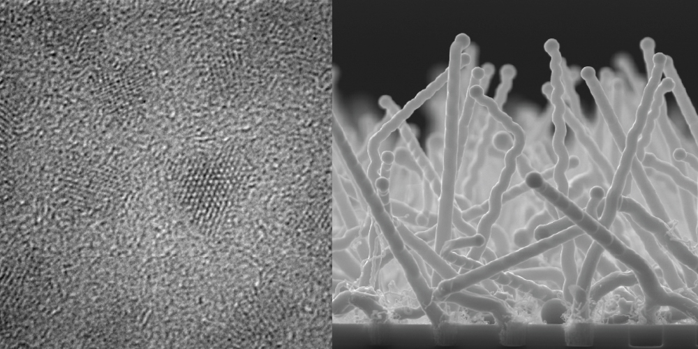
We love nanomaterials! Since our beginning, our group has worked on the preparation and analysis of nanostructured materials. In the context of solar energy, high aspect ratio, crystalline semiconductor nanomaterials (e.g. semiconductor macroporous films, nanowires, quantum dots) are attractive. Judicially designed semiconductor nanomaterials can be enabling components in high efficiency, low cost energy storage technologies. To this end, we have long sought and used various synthetic methods (electrochemical etching, CVD, electrodeposition) to prepare nanomaterials of interest. For nanowires, our group has targeted electrodeposition as a scalable, non energy-intensive strategy for synthesizing crystalline inorganic semiconductor nanowires. We have devised new electrochemical methods that yield fully crystalline group IV and III-V semiconductor materials (e.g. Si and GaAs) directly at low temperatures with minimal energy input.
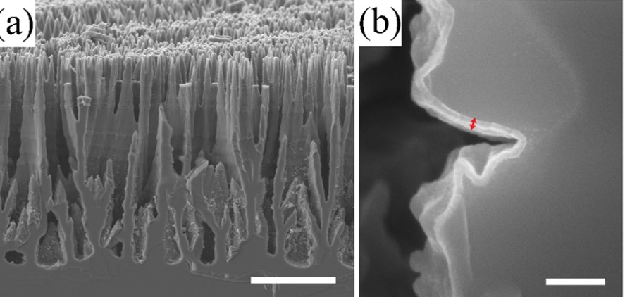 An interesting methodology to make high aspect ratio semiconductor nanomaterials is the anodic etching of semiconductor wafers. Under certain conditions, it is possible to etch wafers selectively so that the remaining material is in the form of thin nanowires. Under other conditions, electrochemical etching can yield macroporous films where the structure of the pore walls can have either straight or highly branched forms. In combination with coating strategies, it is possible to make complex electrode architectures that are well suited for solar energy conversion. An example is shown to the left, where a macroporous GaP film is shown. As prepared, the surfaces of the GaP pores are riddled with defects/dangling bonds/oxide(s). However, atomic layer deposition makes it possible to conformally coat these materials with a thin layer of oxides that then defines the interfacial character of the pores. Changing the oxide layer composition affords another level of tunability for these nanomaterials.
Relevant Publications For More Reading: #57,#22, and #59
Electrosynthesis
An emergent challenge in the 21st century is shifting to carbon neutral energy. While solar energy holds the greatest promise for generating grid-scale renewable energy, overcoming the high production cost of photovoltaic devices with new, low cost synthetic strategies is required. Conventional single crystal semiconductor synthesis requires high temperatures, corrosive reagents, and enormous infrastructural development. Conversely, electrodeposition is attractive for synthesis, as it uses an external bias (rather than a thermal input) and affords excellent temporal and kinetic control. However, due to the insolubility of covalent semiconductors in aqueous and organic media, almost all reports of low temperature electrodeposition of Groups IV and III-V semiconductors describe the generation of amorphous materials.
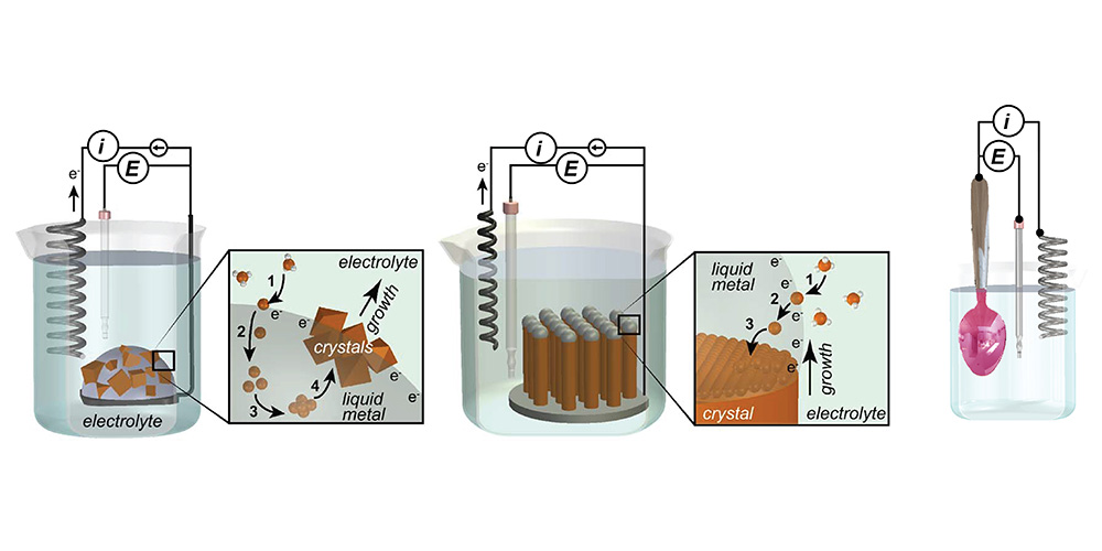
 Our group has recently developed the electrochemical liquid-liquid-solid (ec-LLS) process which uses liquid metal electrodes both to reduce oxidized metal precursors in solution but also a solvent medium for recrystallization of deposited nuclei. Using ec-LLS, we have grown bulk crystals, nano- and micro-wires, and epitaxial thin films of inorganic materials. This technique is one of the few known methods to produce highly crystalline materials at near ambient conditions on the bench-top. At present, we are investigating the fundamental parameters affecting crystal growth by ec-LLS and developing advanced strategies to fabricate devices by this method. A particularly exciting approach is the combination of ec-LLS and conventional liquid phase epitaxy (LPE) in a process we call ec-LPE. Though seldom researched anymore, LPE was invented to create the first generation of III-V and heterostructures devices, which then-contemporary methods could not. Films grown by LPE showed near-perfect to perfect epitaxial quality, owing to the near-equilibrium conditions of the growth mode, in addition to remarkably fast growth rates (0.01 to 1 um min-1) and the high purity material quality. Despite the incredible materials developed using LPE, it has since faded into obscurity among the many methods to make semiconductors owing to its inability to produce arbitrarily thick films and the cumbersome technical set-up it requires. However, by marrying conventional electrodeposition methods with LPE, it is our hope that we can overcome these fundamental limitations, to generate high fidelity and high quality epitaxial thin films, most critically, at low temperature. This approach makes it possible to synthesize semiconductor epifilms in an entirely different way than ever considered before and opens up possibilities in semiconductor research, which have been heretofore impossible. In addition to the research advancements this methodology may bring, the cornerstone hope is that this low temperature method can lead to ultra low cost photovoltaics, detectors, and electronics will retaining good material quality.
A second interest has been to develop electrodeposition methods for obtaining films with desirable properties. An interesting application is in coloring of metals. Rather than use paint or ink, it is possible to use optical interference patterns from a structurally complex thin, overlayer film as a means to impart color on a substrate. Metal-dielectric-metal (MDM) films are one such overlayer. Through judicious control of electrodeposition parameters, it is possible to create ultra thin, smooth MDM stacks that can be used to generate any color imaginable, even on curved metal objects like spoons!
Relevant Publications For More Reading: #52 and #58
Photoelectrochemistry
Inarguably, the simplest design for an artificial photosynthetic system is the immersion of a semiconductor electrode in a beaker of water. Such a construct can have all the functionality of natural photosynthesis but with the potential for producing chemical fuels of interest at much higher yields. This allure has driven the field of photoelectrochemistry for the better part of the last half century. The simplicity of such systems belie the fact that it is difficult to construct a semiconductor for this purpose that is simultaneously cheap, stable in water, and efficient for desirable fuel-forming processes. To this end, our group is intersested in understanding and designing more suitable semiconductor/electrolyte interfaces. Understanding the operation of a semiconductor photoelectrode encompasses many different topics including materials science, device physics, thermodynamics, and reaction kinetics.
One strategy our group has had a long standing interest in is dye-sensitized photoelectrodes. The current dogma for the design of dye-sensitized photoelectrochemical cells consists of five nearly immutable features: (1) wide bandgap metal oxides, (2) panchromatic dyes that overcome the minimal sunlight absorbance by metal oxides like TiO2, (3) charge injection of photoexcited electrons from an excited chromophore into an n type semiconductor immersed in a non-aqueous solution, (4) sunlight to electricity conversion, and (5) ultra-small semiconductor nanoparticles that provide a large surface area for dye loading but are too small to support appreciable internal electric fields.
 We are interested in an alternative direction in dye-sensitized photoelectrochemistry: dye-sensitized photocathodes. Our current efforts in this area are focused on sensitized III-V semiconductors such as gallium phosphide (GaP) photoelectrodes which have several properties advantageous for study. First, GaP can be prepared/obtained with well-defined bulk optoelectronic properties (e.g. mobility and dopant density) that are favorable for efficient light-harvesting systems. Second, dye-sensitized p GaP can support substantial levels of light-stimulated hole injection. High internal quantum yields are attainable with p-GaP photoelectrodes specifically operating under depletion conditions (i.e. featuring a large internal electric field). Third, the response characteristics of planar p-GaP photoelectrodes operating under depletion conditions can be readily modeled and understood using finite-difference simulations, offering the opportunity for detailed analysis. Fourth, as a midsized bandgap semiconductor, GaP can absorb light at wavelengths shorter than 550 nm, relaxing the required panchromaticity of a sensitizer for complete absorbance of sunlight.
Through careful control of the shape and surface chemistry of GaP, it is possible to design sensitized photocathodes. We have shown previously that nanostructuring GaP increases the collection of minority carriers without needing a change in the bulk properties. Combining this tactic with chemical strategies to covalently attach molecular or quantum dot chromophores is our long term goal.
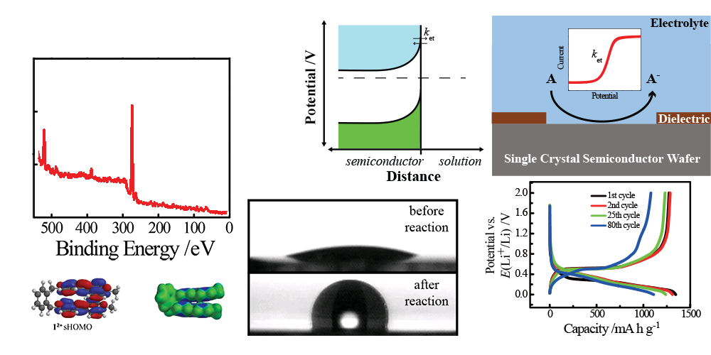
A related interest of our group is the development of semiconductor/water interfaces that are more stable. Through a combination of wet chemical surface functionalization, electrodeposition, and vapor phase treatments, we are investigating new ways to stabilize these interfaces in order to prevent desctructive oxidation/corrosion/dissolution. Along these lines, we have ongoing research projects dedicated to performing reactions on/with semiconductor surfaces that utilize XPS, reflectance IR, Raman, and scanning wavelength ellipsometry.
Relevant Publications For More Reading:#56 and #68
Physical Electrochemistry
Our group is generally interested in developing strategies to study electron transfer between an electrode and molecules in solution. Historically, we have utilized a variety of hybrid spectroscopic methods including SERS, XPS, and UV-Vis reflectance as well as several electroanalytical methods/tools (voltammetry, chronoamperometry, rotating disks, microelectrodes, impedance spectroscopy) to study such processes. These investigations have focused on a variety of topics including chemisorption on ultra-thin semiconductor films, the capacity of rechargeable Li+ battery anodes, alloying reactions between surface atoms and metal electrodes, and identifying the properties of chemically modified semiconductor electrodes.
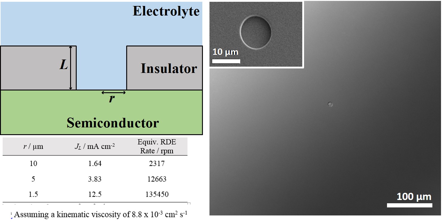 A more recent objective has been to study heterogeneous charge-transfer at semiconductor/liquid interfaces in detail. Towards this goal, we have become interested in semiconductor ultramicroelectrodes (SUMEs). The premise is that miniaturizing the electrode area may substantially simplify the many convoluted features in cyclic voltammetry with semiconductor macroelectrodes. Simply, shrinking the electrode ought to make the interpretation of observable current-potential responses tractable and informative. This motivation is distinct from the extensive literature on metal UMEs and interestingly has been under developed for semiconductors. In this regard, we are actively making SUMEs that push the boundaries of what is possible to fabricate so as to allow full tests of microscopic theories of charge transfer. Our hope is that SUME platforms can become generally useful to the community at large.
In the context of energy conversion systems, we also are interested in identifying new and more optimal ways to load molecular species of interest onto electrode surfaces. A new approach we are exploring involves fabricating ultra-thin reduced graphene oxide films as coatings that readily afford adsorption by aromatic catalysts and/or chromophores.
Relevant Publications For More Reading:#66 and #69
In-Situ Electron Microscopy
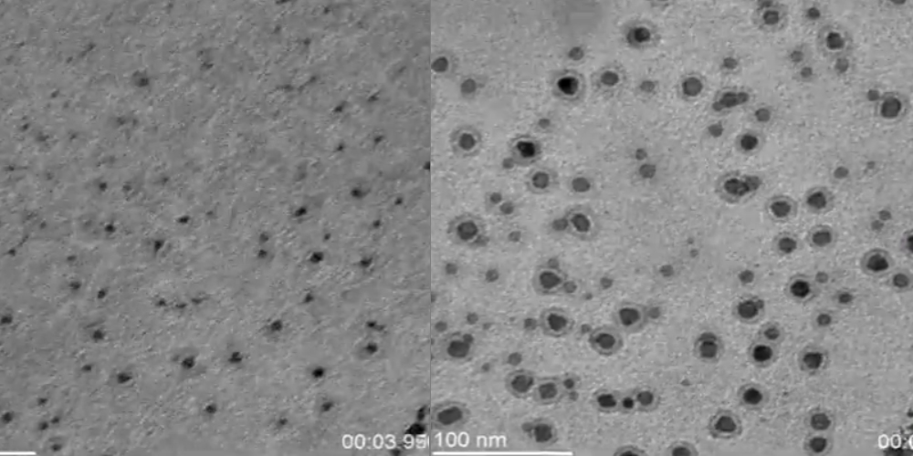
 Electron microscopy is a technique which uses high energy electrons to visualize materials from the microscale to the nanoscale. In Transmission Electron Microscopy (TEM) the electron beam is transmitted through the sample and onto a detector below. In order to maintain a coherent beam of high energy electrons, high vacuum is required in order to maintain a long mean free path for the electrons. In recent years, significant advancements in microfabrication have enabled the ability to create thin cells to separate liquid media from the high vacuum in the TEM while still allowing for transmission of the beam. with these cells, it is possible to perform in-situ liquid TEM experiments. A primary focus of our group is the use of in-situ TEM to study electrochemical reactions with high spatial and temporal resolution.
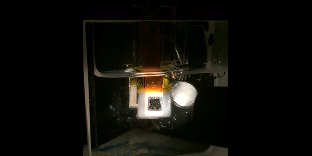
Electroanalytical measurements performed inside a transmission electron microscope (TEM) are rapidly gaining favor for studying electrochemical reactions/systems. The premise is simple. If an electrochemical reaction/measurement is performed inside a thin film cell with windows that permit transmission of a focused electron (e-) beam inside a TEM, then classical electroanalytical measurements can be performed in conjunction with and correlated to imaging and diffraction data at the nanoscale with high spatial and temporal resolutions. This simultaneous approach has already provided new insights on the dynamics and structural changes in electrodes in such diverse processes as lithium ion insertion/deinsertion, metal nucleation during electrodeposition, dendrite formation, and metal corrosion.
Despite the power of the approach, hybrid liquid electrochemical-TEM measurements can be challenging to interpret. The possibility that the electron (e-) beam used in TEM for imaging can induce reactions in liquid solvents, e.g. generation of solvated electrons, free radical generation, and other reactive molecular species, exist. Although complex, these experimental artifacts are similar to phenomenon that occur in techniques such as pulse radiolysis. Accordingly, their effects on measurements can be understood, anticipated, and even leveraged.
There has also been a general recognition that electrochemical data recorded in a TEM can be influenced by either the thin space required to transmit the e- beam or by the presence of the e- beam itself on/near the electrodes. The former point relates to the well-described importance of electrolyte volume and electrode placement in thin-layer electrochemistry. However, the exact origins of how and to what extent the e- beam can alter electrochemical measurements of interest is unclear. Potential measurement artifacts could arise from several sources in hybrid electrochemical-TEM experiments. (1) Electrochemical TEM experiments involve measurements with coupled instrumentation, each with (possibly) different definitions of ground. Ground loops are possible that could introduce measurement noise. (2) The actual area of the electrodes exposed to solution can be very different from the area probed by the e- beam. (3) Absorption of the e- beam of the TEM by an electrode could change the average density of transferrable electrons in the material and thereby alter its measured potential. We are interested in deconvoluting these aspects and more precisely defining the possibilities afforded by in-situ TEM electrochemistry.
Relevant Publications For More Reading: #62
