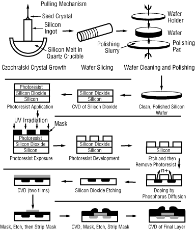
As discussed in Section 6.6, CVD is a very important process in the microelectronics industry. The fabrication of microelectronic devices may include as few as 30 or as many as 200 individual steps to produce chips with up to 10 6 transducers per chip. An abbreviated schematic of the steps involved in producing a typical computer chip is shown in Figure CD12-12.
Although we will focus on CVD, it is worthwhile to give an overview of microelectronic fabrication. Starting from the upper left we see that single crystal silicon ingots are grown in a Czochralski crystalizer, then sliced into wafers, and chemically and physically polished. These polished wafers serve as a starting material for a variety of microelectronic devices. A typical fabrication sequence is shown for processing the wafer beginning with the formation of an SiO 2 layer on top of the silicon. The SiO 2 layer may be formed either by oxidizing a silicon layer or by laying down a SiO 2 vapor deposition (CVD). Next the wafer is masked with a polymer photoresist (PR), a layer by chemical template with the pattern to be etched onto the SiO 2 layer is placed over the PR, and the wafer is exposed to ultraviolet irradiation. If the mask is a positive PR , the light will cause scission in the polymer so that the exposed areas will dissolve when the wafer is placed in the developer. On the other hand, when a negative PR mask is exposed to ultraviolet irradiation, cross-linking of the polymer chains occurs and the unexposed areas dissolve in the developer. The undeveloped portion of the PR (in either case) will protect the covered areas from etching. 
Figure CD12-12
Microelectric Fabrication Steps
After the exposed areas of SiO 2 are etched to form trenches (either by wet etching (see Problem P5-12) or plasma etching), the remaining PR is removed. Next the wafer is placed in a furnace containing gas molecules of the desired dopant, which then diffuse into the exposed silicon. After diffusion of dopant to the desired depth in the wafer, it is removed and then covered with SiO 2 by CVD. The sequence of masking, etching, CVD, and metallization continues until the desired device is formed. A schematic of a final chip is shown in the lower right-hand corner of Figure CD12-12.
One of the key steps in the chip-making process is the deposition of different semiconductors and metals on the surface of the chip. This step can be achieved by CVD. CVD mechanisms were discussed in Chapter 10. Consequently, this section will focus on CVD reactors. A number of CVD reactor types have been used, such as barrel reactors, boat reactors, and horizontal and vertical reactors. A description of these reactors and modeling equations is given by Jensen.26
R12.4-B Fundamentals of CVD
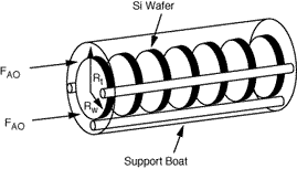
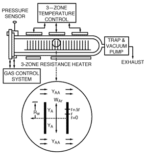
One of the more common CVD reactors is the horizontal low-pressure CVD (LPCVD) reactor. This reactor operates at pressures of approximately 100 Pa. The main advantage of the LPCVD is its capability of processing a large number of wafers without detrimental effects to film uniformity. Owing to the large increases in the diffusion coefficient at low pressures (recall Table 11-2), surface reactions are more likely to be controlling than mass transfer. A schematic of a LPCVD boat reactor is shown in

Figure CD12-13
LPCVD boat reactor
sequence in silicon
deposition

The corresponding rate law is


 SiH 2 .
The reacting gas flows through the annulus between the outer edges of the cylindrical wafers and the tube wall (see Figure CD12-14). The corresponding cross-sectional area of the annulus is
Flow in the
annulus


Figure CD12-14
LPCVD boat reactor with peripherals
R12.4-C Effectiveness Factor for a LPCVD Reactor
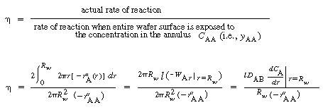
Silicon will deposit on the wafers, the reactor walls, and on the boat support. Deposition on the walls and support will take place at the reactant concentrations in the annulus. However, the concentration of A between the wafers is less than the concentration in the annulus. Consequently, the rate of deposition on the wafer will be less than the rate at conditions in the annulus. Fortunately, these two concentrations can be related by the effectiveness factor. We can determine the effectiveness factor once the concentration profile in the region between the wafers is obtained.

 is the rate of disappearance of A at the concentration of A in the annular region, C AA . We now use
 to express the actual rate of reaction per unit surface area of wafer in terms of the rate of reaction at conditions in the annulus:


