| Select Chapter >> | TOC | Preface | 1 | 2 | 3 | 4 | 5 | 6 | 7 | 8 | 9 | 10 | 11 | 12 | 13 | 14 | 15 | 16 | 17 | 18 | Appendices |
Chapter 10: Catalysis and Catalytic Reactors
The following information is taken from the 4th edition of Elements of Chemical Reaction Engineering, so the equation numbers correspond to those found in that bookR10.4 Etching of Semiconductors
| We have seen in Figure 10-20 that etching (i.e., the dissolution or physical or chemical removal of material) is also an important step in the fabrication process. Etching takes on a priority role in microelectronics manufacturing because of the need to create well-defined structures from an essentially homogeneous material. In integrated circuits, etching is necessary to remove unwanted material that could provide alternative pathways for electrons and thus hinder operation of the circuit. Etching is also of vital importance in the fabrication of micromechanical and optoelectronic devices. By selectively etching semiconductor surfaces, it is possible to fabricate motors and valves, ultrasmall diaphragms that can sense differences in pressure, or cantilever beams that can sense acceleration. In each of these applications proper etching is crucial to remove material that would either short out a circuit or hinder movement of the micromechanical device. |
||
A. Dry EtchingDry etching involves gas-phase reactions (usually in plasmas) that form highly reactive species that impinge on the surface to react with the surface, to erode the surface, or both. In the fabrication of optoelectronic devices, dry etching is used almost exclusively. Indium phosphide (InP) is a material that is used in the fabrication of optoelectronic devices, but it is an extremely difficult material to etch. |
||

|
|
|
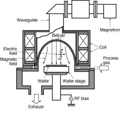
| A schematic of the plasma is shown in Figure R10.3-1. |
||
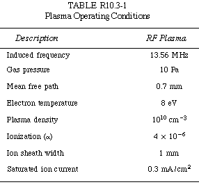
Typical operating conditions are shown in Table R10.3-1. |
||
|
||
|
||
|
||
|
|
||
|
||
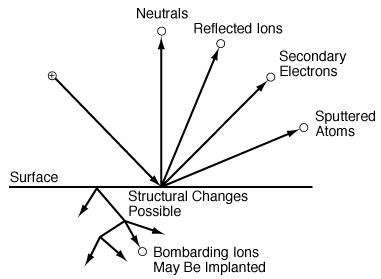
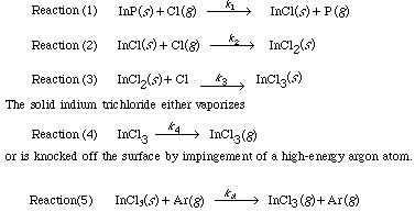
The more volatile InCl 3 is removed from the surface either by argon or by vaporization ion bombardment (Figure R10.3-4). Because a reaction takes place before removal of the material it is called reactive ion etching. We shall now consider the RIE of InP in more detail. This last step is a sputtering reaction.
|
||
|
||
|
||
| (R10.3-1) |
||
| where (Ar) is the concentration of argon above the surface and Net Rate of Formation of Reactive Intermediates. The chemical species InCl and InCl 2 are unstable reactive intermediates. Because the etching takes place at steady state, there is no net rate of formation of these species. That is, they react virtually as fast as they are formed. For Reactions (1) and (2), which are elementary, the net rate is |
||
|
|
(R10.3-2) |
|
Solving for the fraction of the surface covered by InCl gives |
||
|
|
(R10.3-3) |
|
|
|
|
|
||
| (R10.3-5) |
||
|
||
|
(R10.3-6) |
|
|
||
|
|
(R10.3-7) |
|
|
||
|
|
(R10.3-8) |
|
|
||
|
|
(R10.3-9) |
|
|
||
|
|
(R10.3-10) |
|
|
||
|
|
(R10.3-11) |
|
| where |
||
|
|
||
|
||
|
||
Consequently, for all practical purposes the etch rate can be written as |
||
|
|
(R10.3-12) |
|
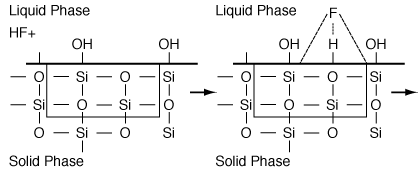
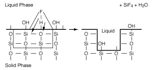
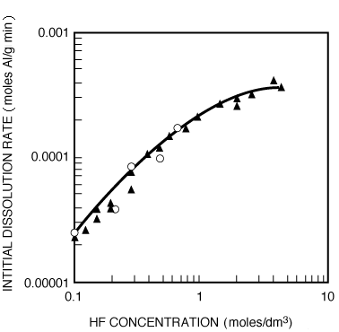
B. Wet Etching Wet etching is used primarily in micromachining, where acids are used to dissolve the solid substrate to form intricate channels and slopes, but it has also been used in the fabrication of computer chips. Figure R10.3-6 shows a schematic of the etching process of material A. When a chemical etch is to be carried out, the portion of the material that is not to be etched is covered by a polymer coating called a photoresist, which prevents it from contacting the acid. |
||
|
||
|
||
|
||
|
||
|
||
The symbol S in this reaction represents the new substrate surface that has been exposed to acid after the layer above it has been removed. As with catalytic reactions, the surface reaction is most often rate-limiting, in which case we have |
||
|
|
(R10.3-13) |
|
|
||
|
|
(R10.3-14) |
|
|
||
|
|
(R10.3-15) |
|
|
||
|
|
(R10.3-16) |
|
|
||
|
|
(R10.3-17) |
|
|
||
|
|
(R10.3-18) |
|
|
||
|
|
(R10.3-19) |
|
|
||
|
|
(R10.3-20) |
|
|
||





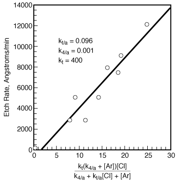
 and dividing by k 1 , the etch rate law for RIE of indium phosphide becomes

